A homebrew Z80 microcomputer
Wenzel Jakob, May 2003
Overview
A month ago, I decided to design and build a custom Z80 microcomputer. This surely was a lot of fun, so I decided to post a step-by-step description along with construction plans for those who might be interested in doing something similar. Click on any picture to open bigger versions.
The Z80 processor was originally developed by Zilog, Inc. In relation to the total market size at the time, is was the most successful microprocessor ever. Today, it is still very popular and commonly used in embedded systems [Source: Wikipedia]. It is available at a reasonable price and uses a DIP socket, which makes it a perfect choice for this project.
My feature wish list for the board was as follows:
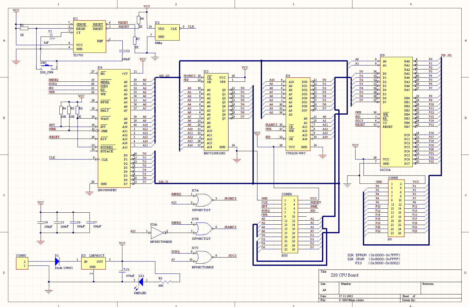
- 32KB ROM in the form of an UV-erasable EPROM
- 32KB static RAM
- 4Mhz system clock. Actually, Z80-Processors work with up to 20Mhz these days—however, for nostalgic reasons, these obviously cannot be used ;).
- Parallel I/O interface
- Reset button
- Reset circuitry, so that the system powers up in a well-defined manner
- Voltage regulation and reverse polarity protection
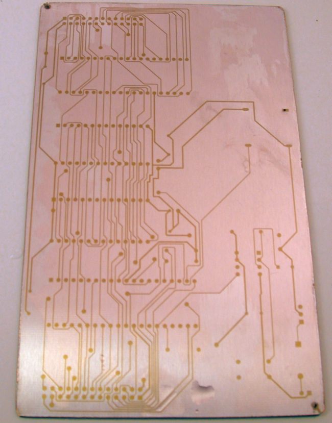
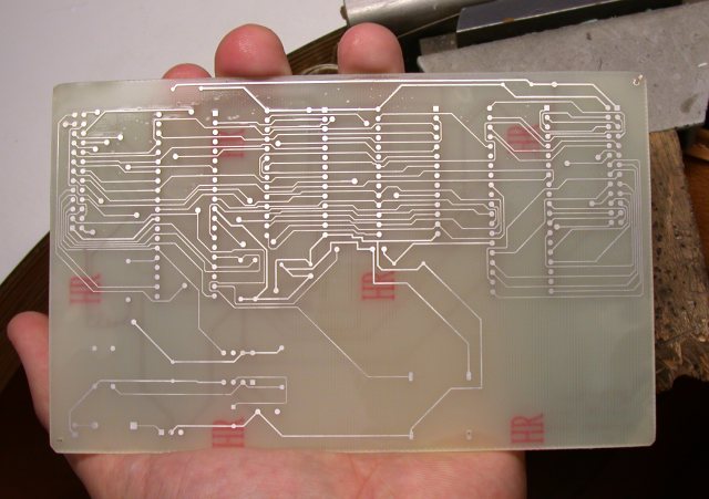
Based on these plans, I designed a schematic and (after much fiddling) managed to turn it into the following sufficiently sane two-layer board layout:
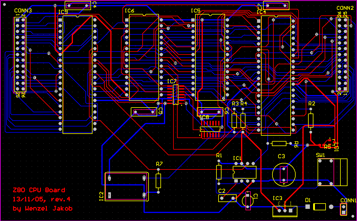
There are also PDF files of the schematics and the board layout.
Exposure
For the exposure, I printed the board layout on standard InkJet transparency film. I had to try out lots of different printer settings since the layer of black ink needed to be absolutely opaque. I ended up having to "lie" to the printer (choosing the 'glossy photo paper' setting despite not using paper at all) so that it would put down enough ink for the next step to work.
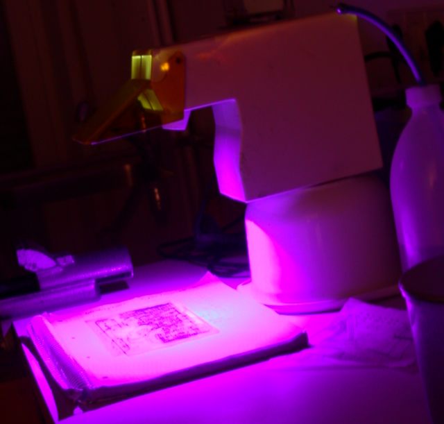
I then put the transparent sheet onto a photo-sensitve board ("photo-resist" PCB) and exposed it to UV light for 6-7 minutes, although this really depends on the type of ultraviolet light source, the board material and especially distance between the two (the exposure time rises quadratically with linear distance increments).
Because the board needs tracks on both sides, the transparency film has to be carefully aligned. I did this by placing two unused pads onto the upper left and lower right side, drilling through them and then using needles to stabilize the construction.
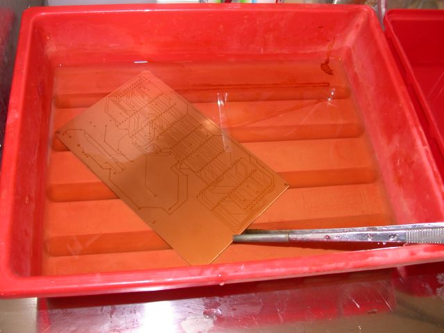
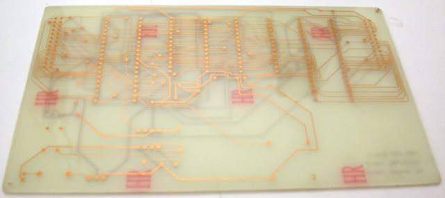
Developing
Diluted sodium hydroxide solution (protective goggles, gloves!) can be used to develop the board. It is important to keep this step as short as possible - otherwise, traces might become too thin.
A closeup picture of the circuit board - one can clearly see how the lacquer layer has been removed on the exposed parts of the board.
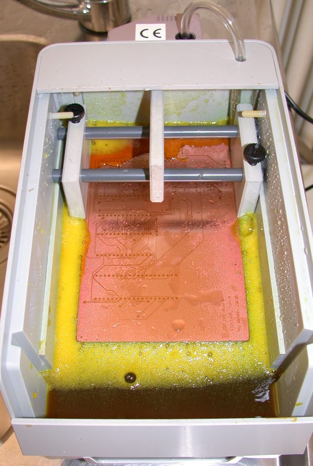
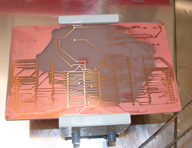
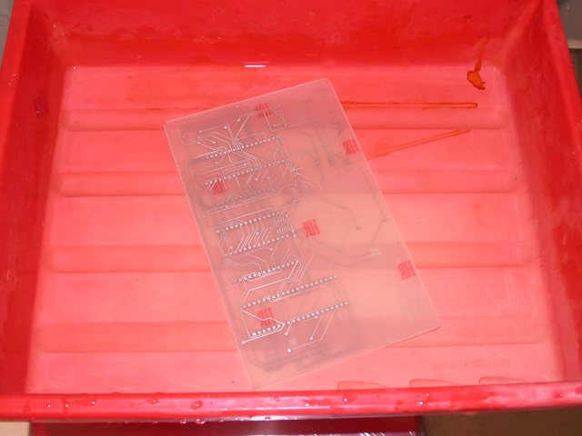
Etching
The etching process was performed using a foam-etching machine and Iron(III)-chloride (600g/1 liter). If the board starts to look like on the second picture, the etching process is almost done.
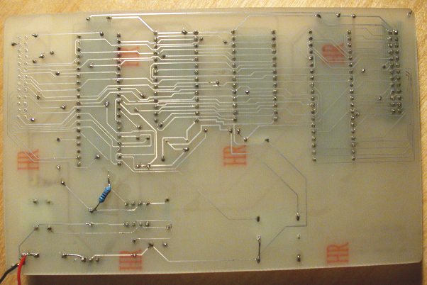
Tin-plating
A tin-plating step is optional, but very advisable since the bare copper will oxidize within days. Additionally, the tin layer makes soldering the board much easier. I used the galvanic tin-plating solution available here and recommend it because it works without electrolysis.
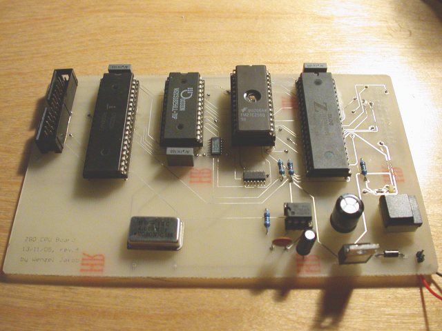
Assembly
A bill of materials and assembly diagram documents are available here and here. For the most part, soldering is relatively simple. Soldering the surface mount components takes some practice. Note: The photograph shows an extra resistor on the bottom, which is not needed by the latest revision of the schematic and layout on this page.
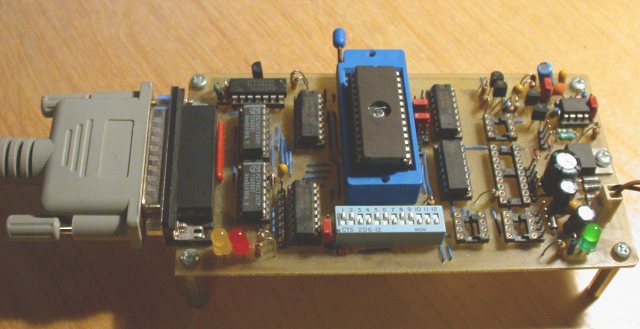
Programming
To fill the EPROM on the board with content, some kind of programming tool is also necessary. I built the one shown below, which can be hooked up to the parallel port of a computer (but generally it may be easier to just buy one that works over USB).
Since building the Z80 board, I also made a periphery board providing a hex keyboard and 4x20 LCD display so that it is possible to get visual feedback more easily (debugging programs by looking at an oscilloscope is no fun at all). The latest version of the board described on this page works nicely, and I have not needed to make further revisions.